I didn’t see a computer for the first time until I was in sixth grade. The most surprising thing to me at that time was the long start-up process it took. It would scroll across the screen and display various letters that I did not know. When I went to university, as I was not a computer science student, I only studied operating systems and programming languages, but not the principles of computer composition systematically. After working, I seldom needed to use this knowledge. Therefore, my understanding of this issue is still very vague. Recently, I read an article by Hackman, which briefly introduces the boot process of early computer hardware, although it is a bit outdated, the basic principles are still similar to those of modern CPUs. Today I am sharing my study notes with you.
The CPU is usually reset when the computer is powered on; the CPU chip has a special reset pin, called RESET or RST, which is set to high when the motherboard is powered up, and the CPU receives the signal to initialise the various states.
One question here is why the CPU does not work directly after booting, but needs to be reset; Hackman’s explanation is also interesting. He says that the motherboard generates a ‘dirty current’ when it is powered up. Dirty in this case can be interpreted as an unstable voltage at the moment of power-on. The digital circuits used in computers have certain requirements for voltage ranges, so unpredictable states can occur.
This is rather general, so I’ll add a specific example of why the circuit is in an unknown state after power is applied.
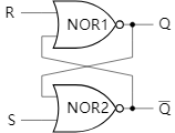
The diagram below shows the schematic of the R-S flip-flop, which I am sure is not new to you. The R-S flip-flop and its derivative circuits are used extensively within computers.
The truth table for the R-S flip-flop is as follows:
| S | R | Q | $\bar{Q}$ |
|---|---|---|---|
| 1 | 0 | 1 | 0 |
| 0 | 1 | 0 | 1 |
| 0 | 0 | Q | $\bar{Q}$ |
| 1 | 1 | - | - |
The R-S flip-flop can save the last state set. This means that as long as S goes high, Q will remain high unless R is set high to reset the state. If S and R are both low, then Q stays the same.
Now the question arises. For the R-S flip-flop, what is the state of Q after the first power-up? The answer is indeterminate. It could be high or it could be low. Look at the circuit diagram above. Theoretically both S and R are low. If NOR1 goes high first, then NOR2 must go low, which will lock Q high; conversely, if NOR2 goes high first, then Q will lock low.
In order for the computer to work properly, it is necessary to actively set R high to complete the initialisation. After the reset Q must be low.
The reset process lasts for a second or two, after which the motherboard resets the RST pin to low and the CPU starts working normally.The work of the CPU can be simply understood as the execution of a series of instructions in memory, all CPUs are constantly fetching the corresponding instructions from memory and then executing them.
The memory here consists of RAM and ROM; ROM is stored in a special chip on the motherboard and will not be lost even after a power failure; RAM is often referred to as a memory stick, which is used for temporary storage of data and instructions and will be cleared after a power failure. When the system starts up, the CPU will first execute the instructions in the ROM, and the CPU uses the address bus to read the memory data. The address is the memory number and the CPU needs to write the corresponding address to the address bus in order to read the memory data of a certain address.
So where in memory is the first instruction executed by the CPU? Different CPUs have different ways of handling this. Some will execute the instruction directly at a specific address, while others use so-called reset vectors, which check a particular section of memory first and then load the instruction at a different memory address depending on the result.
For example, the Z80 CPU executes the instruction at address 0x0000 first after a reset, which is very simple; the 65025 CPU stores the so-called reset vector in memory at 0xFFFC and 0xFFFD. These two bytes store the memory address of the actual instruction in a little-endian way. If the value of 0xFFFC is 0x00 and 0xFFFD is B0, the 6502 CPU will load and execute the corresponding instruction from 0xB000. This design has two advantages. Firstly, it allows flexibility in controlling the CPU’s execution of instructions, as the engineer can write different addresses to the reset vector according to different conditions, thus controlling the CPU’s behaviour; secondly, it does not occupy the low address space starting at 0x0000. The Z80 solution is relatively simple, but the disadvantage is that the low address space can only be used by ROM.
The CPU has a special register called the instruction pointer, which holds the address of the next instruction to be executed by the CPU. For every instruction executed by the CPU, the IP register is incremented by one. If a JMP instruction is encountered, the CPU writes the target address of the JMP into the IP register and then starts executing the instruction in the memory to which the IP refers. CPU instructions are also called opcodes, which are a specific string of 0s and 1s. For example, on an x86 CPU, 0x90 means NOP, which the CPU encounters and does nothing, then executes the next instruction.
Wherever the CPU loads instructions from, the system must first execute the instructions in ROM. After the computer has booted up, it needs to do some basic checks and initialisation, and these instructions are stored in the BIOS on the motherboard. The BIOS system is the first thing that runs when the computer is powered up.
Once the BIOS has finished executing, the BIOS will decide what further instructions to execute. Typically, the BIOS will find a disk on the system and load a specific sector into memory, and then start executing the instructions inside. This part of the instruction is also commonly called a boot loader, formerly known in the open source world as GRUB. At this point, the BIOS surrenders control of the system. The boot loader loads the corresponding system memory according to the configuration and hands over the CPU to the operating system.
The computer has different memory areas or devices, but only one bus. how does the CPU specify the different devices when accessing memory? The easiest way is to use a conversion chip, such as a 3-8 converter.
We can use three address lines to select different chips. There are eight different combinations of three binary bits: 000, 001, 010, 011, 100, 101, 110, 111. we can convert these eight combinations into eight zero-one signals A0-A7 via the 3-8 converter and connect them to the select pins (CS) of each device, so that different devices can be selected using different addresses.
The schematic diagram of the 3-8 converter is as follows:

Assuming a 16-bit bus, using 3 of these bits to select a device leaves 13 bits available for in-device addressing. This means that each device can support up to 8k of memory, which adds up to 64k of memory. Although this is not comparable to the several gigabytes or even tens of gigabytes of memory available today, this was a lot back then. The corresponding address space was as follows:
These are the main points of this article. In addition to Hackman’s article, I have also referred to the book “Coding: The Language Behind Computer Hardware and Software”. It is also a great book that you will not want to miss. It goes from coding to logic circuits to CPU principles in a step-by-step manner and is very well presented. I’ll be sharing my learning experience in due course, so stay tuned.