The pattern of development of most things in the world is similar. In the beginning, relatively general solutions tend to appear to solve most problems, followed by solutions specifically designed for a certain scenario that do not solve general problems but perform extremely well in some specific areas. In the field of computing, the CPU (Central Processing Unit) and the GPU (Graphics Processing Unit) are general-purpose and specific solutions, respectively, with the former providing the most basic computing power to solve almost any problem, and the latter excelling in areas such as graphics computing and machine learning.
Heterogeneous computing refers to systems that use multiple processors or cores at the same time. These systems improve overall performance or resource utilization by adding different coprocessors, which can be responsible for handling specific tasks in the system, such as GPUs for rendering graphics and ASIC integrated circuits for mining.
The term central processing unit was born in 1955 and has been around for more than 70 years. CPU is a mature technology today, but while it can handle general-purpose computing tasks well, it is far inferior to the Graphics Processing Unit (GPU) in the graphics field because of the limitation of the number of cores. Complex graphics rendering, global lighting, and other problems still require GPUs to solve, and the development of technologies such as big data, machine learning, and artificial intelligence are driving the evolution of GPUs.
Today’s software engineers, especially those in data centers and cloud computing, face more complex scenarios because of the development of heterogeneous computing. In this article, we focus on the evolution of CPUs and GPUs, and revisit what interesting features engineers have added to them over the past decades.
CPU
Higher, faster and more powerful is the eternal quest of mankind, and the progress in technology is no exception. There is really only one main direction of CPU evolution: to consume the least amount of energy to achieve the fastest computing speed, and countless engineers have worked to achieve this seemingly simple goal. In this section we briefly show what technologies have been introduced throughout history to improve the performance of CPUs.
Fabrication Process
When we discuss the development of CPU, Fabrication Process is a keyword, I believe people who do not know about computers have heard of Intel processor 10nm, 7nm process, and various CPU manufacturers have their own roadmap to achieve a smaller process, for example, TSMC is ready to achieve 3nm and 2nm manufacturing process in 2022 and 2023 respectively.
In most people’s eyes, it seems like the less process the CPU has, the more advanced it is and the better the performance will be, but process is not a measure of CPU performance, and at the very least process evolution does not directly improve CPU performance. Each increase in process allows us to fit more transistors per unit area, and only more transistors means more performance.
The smaller the transistor the less energy it consumes to switch on and off, and since the transistor needs some time to charge and discharge, the less energy it consumes and the faster it is, which explains why increasing the voltage of the CPU can increase its speed. In addition, the smaller transistor spacing makes the signal transmission faster, which can also speed up the processing speed of the CPU.
Cache
The cache is also an important part of the CPU that reduces the time it takes for the CPU to access memory, as many developers have seen in the table below, we can see that reading data from the CPU’s level 1 cache is about 200 times better than the main memory, and even the level 2 cache is almost 15 times better.
| Work | Latency |
|---|---|
| L1 cache reference | 0.5 ns |
| Branch mispredict | 5 ns |
| L2 cache reference | 7 ns |
| Mutex lock/unlock | 25 ns |
| Main memory reference | 100 ns |
| Compress 1K bytes with Zippy | 3,000 ns |
| Send 1K bytes over 1 Gbps network | 10,000 ns |
| Read 4K randomly from SSD* | 150,000 ns |
| Read 1 MB sequentially from memory | 250,000 ns |
| Round trip within same datacenter | 500,000 ns |
| Read 1 MB sequentially from SSD* | 1,000,000 ns |
| Disk seek | 10,000,000 ns |
| Read 1 MB sequentially from disk | 20,000,000 ns |
| Send packet CA->Netherlands->CA | 150,000,000 ns |
Today’s CPUs generally contain L1, L2, and L3 caches, and CPU access to these caches is second only to access to registers, which are fast, but because high performance needs to be guaranteed as close to the CPU as possible, it is exceptionally expensive. A larger CPU cache means higher cache hit rates, which also means faster speeds.

Intel’s processors have spent the last few decades increasing L1, L2, and L3 cache sizes, integrating L1 and L2 caches in the CPU to improve access speeds, and differentiating between data and instruction caches in the L1 cache to improve cache hit rates. Today’s Core i9 processors have 64 KB of L1 cache and 256 KB of L2 cache per core, with 16 MB of L3 cache shared by all CPUs.
Parallel Computing
Multi-threaded programming is almost mandatory for engineers today, and the increasing number of CPU cores on mainframes has forced engineers to think about how they can use the hardware to its fullest potential through multi-threading. Many people may think that CPUs execute commands serially as written, but the real reality is often more complex than that, and embedded engineers have been trying to execute instructions in parallel on a single CPU for many years.
From a software engineer’s perspective, we can indeed think of every assembly instruction as an atomic operation, and an atomic operation means that the operation is either in an unexecuted or executed state, and database transactions, logging, and concurrency control are all built on atomic operations. However, if we zoom in again on the execution of the instruction, we see that the instruction execution process is not atomic:

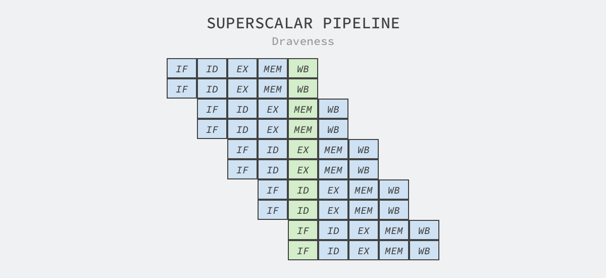
The process of executing instructions varies from machine architecture to machine architecture. The above is a 5-step process of command execution in a classic RISC architecture, which includes fetching instructions, decoding instructions, executing, accessing memory, and writing back to registers.
A superscalar processor is a CPU that can achieve instruction-level parallelism by dispatching instructions to other execution units on the processor to execute multiple instructions simultaneously in a single clock cycle, where the execution units are resources within the CPU, such as arithmetic logic units, floating-point units, etc.
Superscalar design means that the processor issues multiple instructions in a single clock cycle. This technique is often used in conjunction with instruction pipelining, which splits the execution into multiple steps, and different parts of the processor are responsible for the processing of these steps separately, e.g., because instruction fetching and decoding are handled by different execution units, they can be executed in parallel.
In addition to superscalar and pipelining techniques, embedded engineers have introduced more sophisticated techniques such as chaotic execution and branch prediction, where chaotic execution is also called dynamic execution because the CPU needs to load data into registers first when executing instructions, so we analyze the CPU’s register operations to determine which instructions can be executed in chaotic order.

As shown above, it contains three instructions R1 = R0 + R1, R2 = R1 - R0 and R3 = R3 + R5, where the third instruction uses two registers unrelated to the first two, so the instruction can be executed in parallel with the first two instructions, which also reduces the time needed to execute this code.
Because branch conditions are common logic in programs, when we introduce pipelining and chaotic execution in CPU execution, if we encounter a conditional branch and still need to wait for the branch to be determined before continuing to execute the code that follows, the processor may waste many clock cycles waiting for the condition to be determined. In computer architecture, a branch predictor is a digital circuit used to predict the outcome of execution of a condition when a conditional jump instruction is encountered and selects a branch for execution before the branch is determined.
- If the prediction is correct, it saves the clock cycles required to wait and increases CPU utilization.
- If the prediction fails, it needs to discard all or part of the results of the predicted execution and re-execute the correct branch.
Because the failure of the prediction requires a large cost, generally between 10 ~ 20 clock cycles, so how to improve the accuracy of the branch predictor has become a more important topic, the common implementation includes static branch prediction, dynamic branch prediction and random branch prediction.
These instruction-level parallelisms exist only in the implementation details, CPU users will still get the observation of serial execution when observed from outside, so engineers can think of CPUs as black boxes capable of serial instruction execution. To fully utilize the resources of multiple CPUs, engineers still need to understand the multithreaded model and master some concurrency control mechanisms in the operating system.
Single-core superscalar processors are generally classified as Single Instruction stream, Single Data stream (SISD) processors, while if the processor supports vector operations, it is classified as Single Instruction stream, Multiple Data streams (SIMD) processors, and CPU vendors will introduce SIMD instructions to increase the processing power of the CPU.
On-chip layout
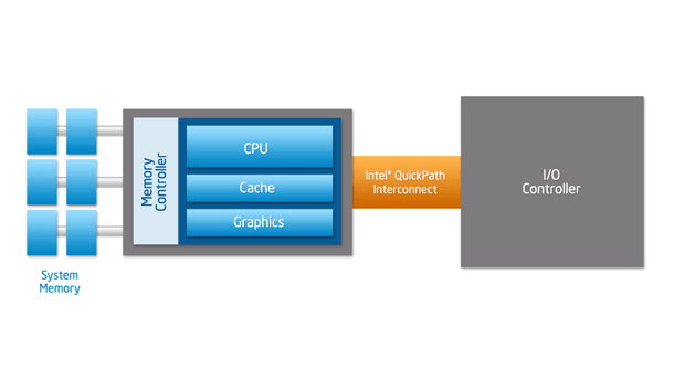
The front-end bus is a communication interface used by Intel in 1990 in chips, and AMD introduced a similar interface in CPUs, both of which serve to pass data between the CPU and the memory controller center (also known as the North Bridge). The front-end bus was not only flexible and inexpensive when it was first designed, but it was difficult to support the increasing number of CPUs in the chip.
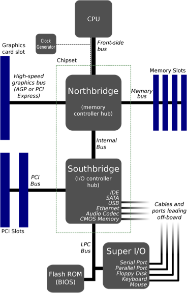
If the CPU can’t get instructions and data from main memory quickly, it will spend a lot of time waiting to read and write data from main memory, so the higher-end processors need high bandwidth and low latency, and the slower front-end bus can’t meet such needs. The Southbridge in the diagram above has been replaced by a new transport mechanism, where the CPU accesses memory via an integrated internal memory control, and connects to other CPUs and I/O controllers via QPI.
Using QPI to allow the CPU to connect directly to other components does increase efficiency, but as the number of CPU cores increases, this connection limits the number of cores, so Intel introduced the Ring Bus in the Sandy Bridge microarchitecture as follows.
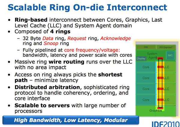
Sandy Bridge introduces on-chip GPUs and video decoders in the architecture, and these components also need to share the L3 cache with the CPU. If all components were directly connected to the L3 cache, there would be a large number of connections on-chip, which is unacceptable to the chip engineers. The on-chip ring bus connects the CPU, GPU, L3 cache, PCIe controller, DMI, and memory, and contains four rings with different functions: data, request, acknowledge, and listen, which reduces the number of connections within different components and provides better scalability.
However, as the number of CPU cores continues to increase, the connections in the ring become larger, which increases the size of the ring and thus affects the access latency between components across the ring, leading to bottlenecks in the design. Intel has thus introduced a new mesh interconnect architecture.
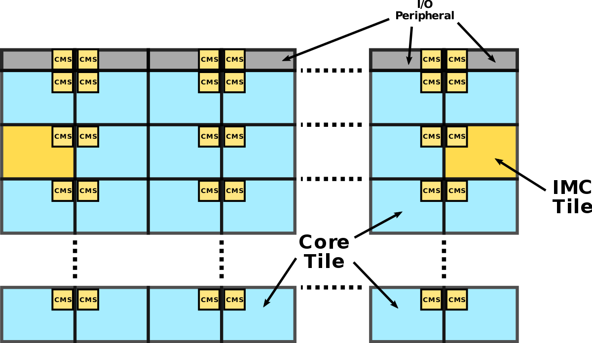
As shown above, Intel’s Mesh architecture is a two-dimensional CPU array with two different components in the network, one is the CPU core in blue in the figure above and the other is the integrated memory controller in yellow in the figure above. These components are not directly connected, but the adjacent modules are connected through Converged Mesh Stop (CMS), which is very similar to the service grid we see today.
When different components need to transfer data, the packets will be transferred by the CMS, with vertical routing followed by horizontal routing, and when the data reaches the target component, the CMS will pass the data to the CPU or the integrated memory controller.
GPU
Graphics Processing Units (GPUs) are specialized circuits that manipulate and modify memory quickly in buffers, and are widely used in embedded systems, mobile devices, personal computers, and workstations because they accelerate the creation and rendering of images. However, with the growth of machine learning and big data, many companies are using GPUs to speed up the execution of training tasks, which is a more common use case in data centers today.
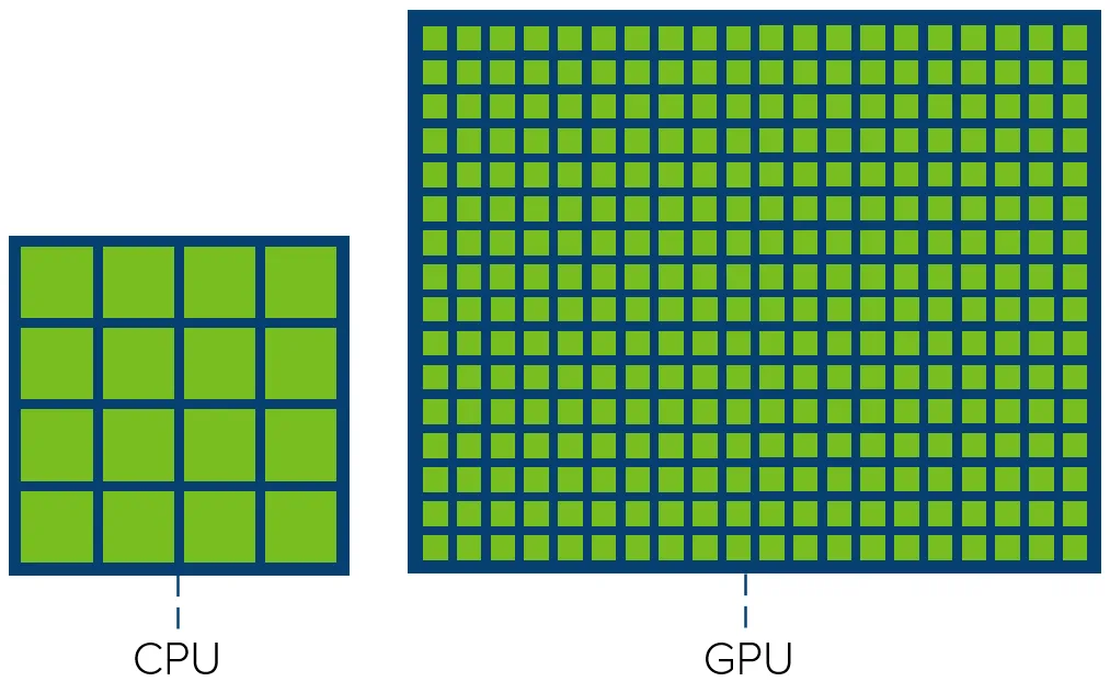
Most CPUs not only expect to complete tasks faster in the shortest possible time to reduce system latency, but they also need to switch between tasks quickly to ensure real-time performance, and because of this need, CPUs tend to execute tasks serially. The difference in design philosophy is ultimately reflected in the number of CPU and GPU cores.
Although GPUs have evolved considerably over the past few decades, the architectures of different GPUs are similar, and we briefly describe here the roles of the different components in the following streaming multiprocessors.
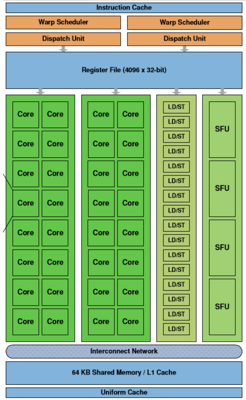
The Streaming Multiprocessor (SM) is the basic unit of a GPU. Each GPU consists of a set of SMs, and the most important structure in the SM is the compute core Core, which in the figure above contains the following components.
- Thread Scheduler (Warp Scheduler): The thread bundle (Warp) is the most basic unit. Each thread bundle contains 32 parallel threads that execute the same command using different data, and the scheduler will be responsible for the scheduling of these threads.
- Access storage units (Load/Store Queues): fast transfer of data between the core and memory.
- Cores: the most basic processing unit of the GPU, also known as Streaming Processor, each of which can be responsible for integer and single-precision floating-point calculations.
In addition to these components, the SM also contains the Special Functions Unit (SPU) as well as the Register File, Shared Memory, Level 1 cache, and General Cache for storing and caching data.
Horizontal Scaling
As with CPUs, increasing the number of cores in an architecture is the easiest and most brutal way to increase GPU performance and throughput, and Fermi, Nvidia’s early graphics processor microarchitecture, contains 16 streaming multiprocessors, 512 CUDA cores, and 3,000,000,000 transistors in the following architecture.
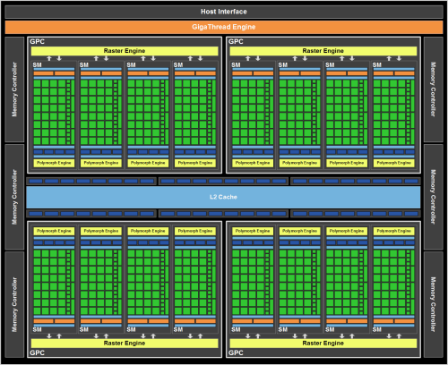
In addition to the 512 CUDA cores, the above architecture contains 256 access storage units for data transfer and 64 special function units. A simple comparison of the Fermi architecture, released in 2010, and Ampere, released in 2020, reveals a huge difference in the number of cores.
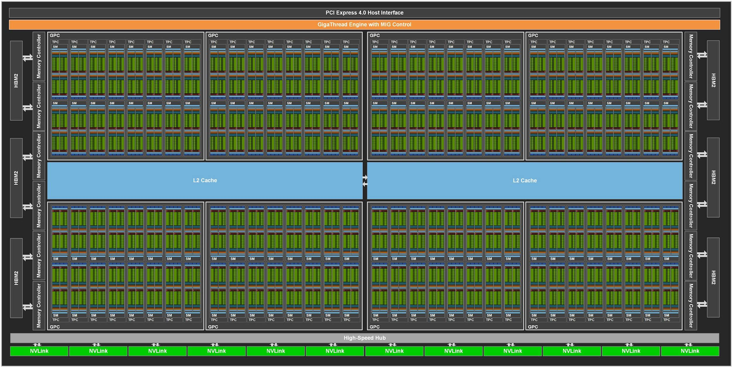
The Ampere architecture has increased the number of streaming multiprocessors to 128 and the number of cores per processor to 64, for a total of 8,192 CUDA cores on the entire card, 16 times the number of cores in the Fermi architecture. To increase system throughput, the new GPU architecture not only has more cores, it also requires more registers, memory, cache, and bandwidth to meet computational and transfer requirements.
Dedicated Cores
Initially, GPUs were only designed to create and render images faster, and they were widely available on personal hosts for image rendering tasks, but as technologies such as machine learning evolved, more kinds of dedicated cores emerged in GPUs to support specific scenarios, and we present here two types of dedicated cores that exist in GPUs: the Tensor Core and the Ray-Tracing Core.

Unlike GPUs on personal computers, GPUs in data centers are often used to perform high-performance computing and training tasks for AI models. It is because of similar needs in the community that Nvidia is adding the Tensor Core18 to its GPUs to specifically handle related tasks.
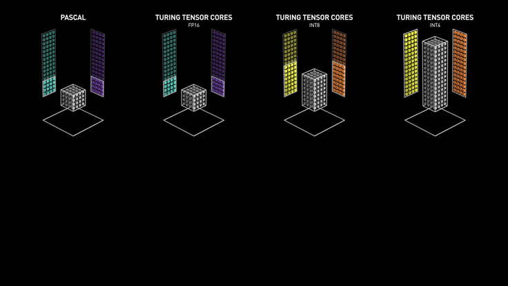
Tensor cores are actually quite different from regular CUDA cores, which can perform exactly one integer or floating-point operation per clock cycle, and the clock speed and number of cores affect the overall performance. The tensor core can perform a 4 x 4 matrix operation at each clock calculation by sacrificing a certain amount of precision, and its introduction makes it possible to perform real-time deep learning tasks in games, enabling accelerated image generation and rendering.
The holy grail in computer graphics is real-time global illumination, where better ray tracing can help us render more realistic images on screen, but global illumination requires a lot of computation from the GPU, and real-time global illumination has very high performance requirements. Traditional GPU architectures are not good at tasks like ray tracing, so Nvidia introduced the first ray-tracing core (Ray-Tracing Core, RT Core) in the Turing architecture.
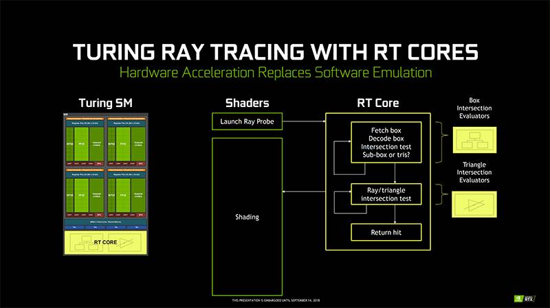
Nvidia’s ray tracing core is actually a special circuit designed for ray tracing. The more common algorithms in ray tracing are Bounding Volume Hierarchy (BVH) traversal and ray triangle intersection tests, which use streaming multiprocessors to calculate the algorithm for each ray that will take thousands of instructions20, and the ray tracing core can speed up the process.
Multi-tenancy
GPUs are very powerful today, but either using GPU instances provided by data centers or building your own servers to run computational tasks is expensive, yet GPU power splitting is still a more complex problem today, running simple training tasks can take up an entire GPU, in which case every little bit of GPU utilization can reduce some costs.
Nvidia’s latest Ampere architecture supports Multi-Instance GPU (MIG) technology, which enables horizontal slicing of GPU resources.21 Each A100 GPU can be split into seven GPU instances, each with isolated memory, cache, and compute cores, which not only meets the data center’s need to divide GPU resources, but also allows for running different training tasks in parallel on the same card. This not only meets the need to split GPU resources in the data center, but also allows different training tasks to be run in parallel on the same graphics card.
Summary
As we can see from the evolution of CPUs and GPUs, all compute units have benefited from more refined manufacturing processes, we tried to put more transistors in the same area and add more compute units and use larger caches, and as this ‘simple and brutal’ approach became more difficult due to physical bottlenecks, we started to design specialized compute units for specific domains.
ASICs and FPGAs, which are not mentioned in the paper, are more specific circuits, and outside of image rendering, we can improve the performance of a task by designing ASIC and FPGA circuits for a specific domain, as shown in OSDI ‘20’s best paper hXDP: Efficient Software Packet Processing on FPGA NICs. The best paper from OSDI ‘20, hXDP: Efficient Software Packet Processing on FPGA NICs, examines how packet forwarding can be handled more efficiently using programmable FPGAs, a task that will increasingly use specialized hardware in the future.