Explore the memory structure of a computer species and how the CPU reads and writes data in memory and how to maintain data consistency in the CPU cache. What is virtual memory and the need for it to exist.
Overview
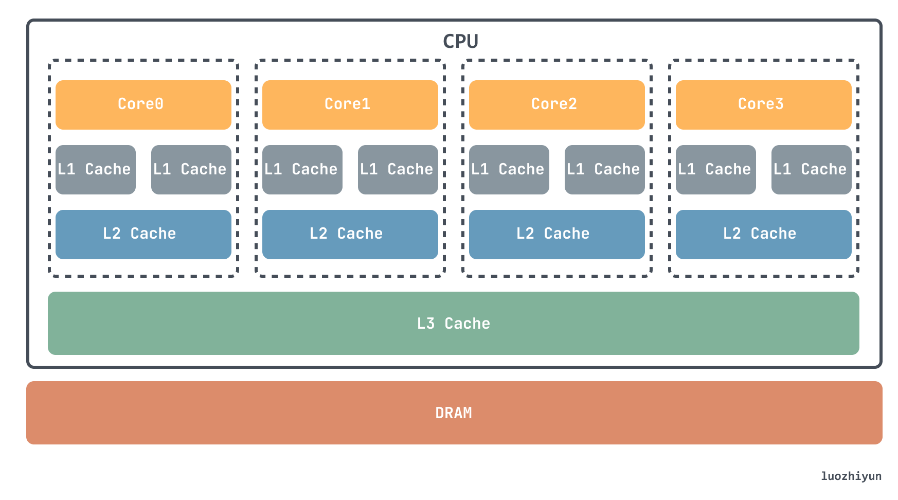
Currently, SRAM is mainly integrated in CPUs, and each CPU core has its own L1 cache, which is usually divided into instruction cache and data cache to store instructions and data used by the CPU separately, while the L2 cache is also available in each CPU core, but it is often not inside the CPU core. Therefore, L2 cache access speed is slightly slower than L1. The L3 cache, on the other hand, is usually shared by multiple CPU cores.
In DRAM, the memory cell uses a capacitor to hold the charge to store the data. The capacitor is constantly leaking, so it needs to be refreshed and charged regularly to keep the data from being lost. Since DRAM requires only one transistor to store one bit, the data stored is much larger.
Let’s look at some of their speeds.
- L1 access speed: 4 CPU clock cycles
- L2 access speed: 11 CPU clock cycles
- L3 access speed: 39 CPU clock cycles
- DRAM memory access speed: 107 CPU clock cycles
CPU cache
cache structure
As we said above, for the CPU, SRAM is called the CPU cache. The CPU accesses the cache every time it fetches data, and loads the data into the cache if it cannot fetch it. Since the size of the cache is much smaller than the main memory, it is also necessary to maintain a mapping relationship between the cache and the main memory so that the data can be found correctly.
One simple way is direct mapping, which is like finding data and putting it directly into a map for storage, where the mapping is modulo the number of addresses and cache to get the address of the main memory in the cache to get the data.
|
|
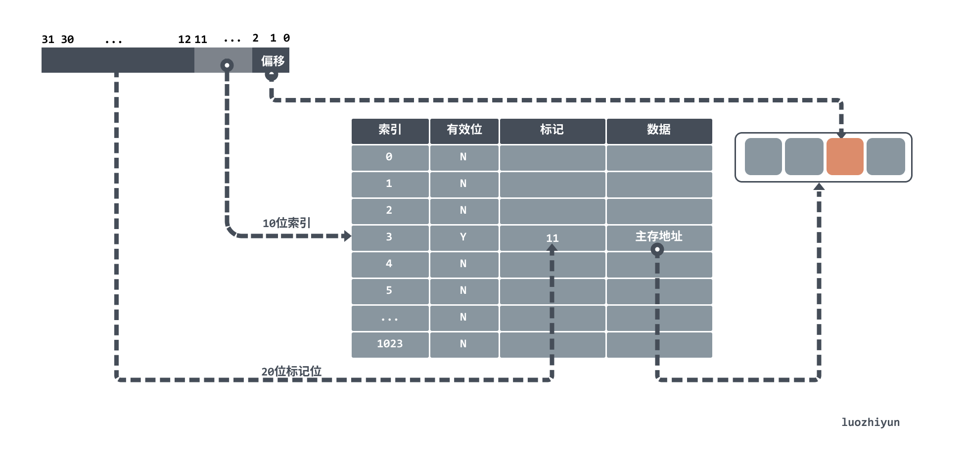
The above diagram shows an address going to the cache. For cache, it can be divided as follows.
- Index: used to take the mode to find the corresponding cache row.
- valid bit: the initial value of the cache is empty at the beginning, this field marks whether the cache row has data or not.
- marker: used to compare with the address whether it is the corresponding data or not.
- Data: indicates the actual data stored, which can be obtained by offsetting the address to the corresponding data.
For example, if the cache has 1024 words, i.e., 4KB, and there is a 32-bit address to find data in the cache, then the 10 bits of the address will be modulo to find the corresponding cache row, and then the 20 bits will be compared with the cahce marker bits, and if they are equal and the valid bits are on, then the corresponding request address is hit in the cache. Otherwise, a miss occurs.
Since the CPU is not reading a whole block of data, but a fragment of data that it needs, the cache will index the corresponding word according to the offset of the lower two bits after the hit.
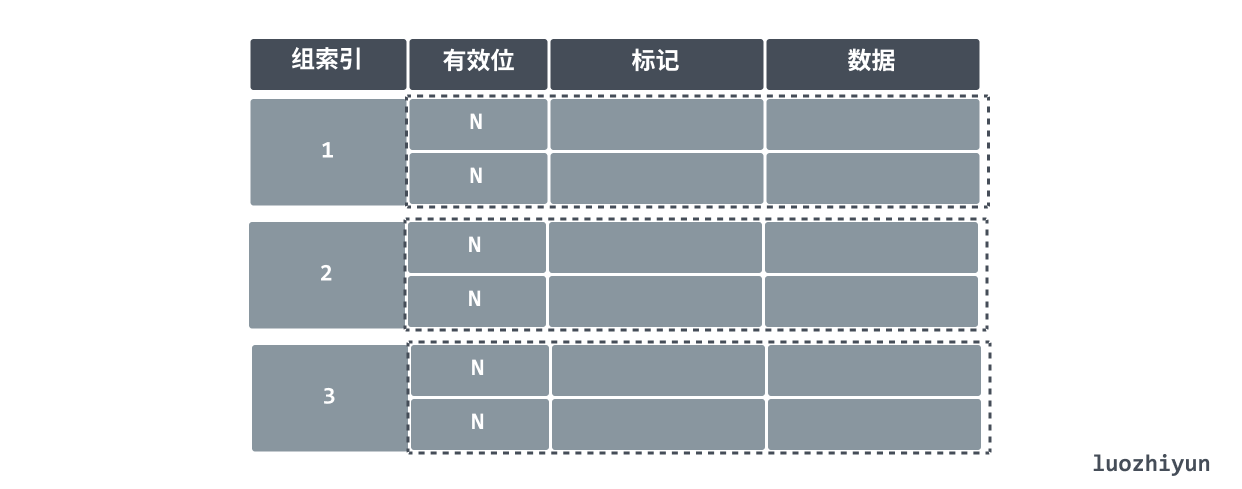
In addition to the direct mapping mentioned above, there are group concatenation and full concatenation.
Group concatenation is the use of group index instead of the original index, the following figure indicates that there are 2 rows of data in each group, find the corresponding data rows by group index and then search for each row in the group by valid bits and tags, if it matches, it means it is a hit.
cache read and write operations
Let’s look at read operations first. cache is empty in its initial state, and reading data at this time will result in a cache miss. cache controller will detect the miss and retrieve the required data from the main memory (or a lower level cache). If it hits, then it will be used directly.
When a cache miss occurs, some other instructions can still be executed for a chaotic execution processor, but for a sequential execution processor, the cache miss is blocked and the contents of temporary registers and registers visible to the programmer are essentially frozen.
Let’s look at write operations. Since the cache is composed of multiple levels, there are generally two write policies: write-through and write-back. These two policies are used to keep the data written in the cache the same as the data in the main memory.
write-through means that the data is written to the main memory immediately after it is written to the cache, but due to the performance difference between the main memory and the cache, it will take a lot of time to write to the main memory each time. The solution is to add a write buffer, so that the CPU can continue execution after writing data to the cache and buffer, and then release the buffer after it is written to the main memory.
However, if the write speed is faster than the buffer release speed, it will still block the CPU execution. Then consider the write back strategy, which writes only the new value to the cache on each write, and writes to a lower-level storage structure only when the modified block is replaced.
Consistency and the MESI protocol
Since there are multi-core CPUs with multiple levels of cache and data sharing, a mechanism is needed to ensure that the cache data seen in different cores must be consistent. The most commonly used protocol to handle cache coherency between multi-core CPUs is the MESI protocol.
The MESI protocol is a protocol called Write Invalidate. In the write invalidate protocol, only one CPU core is responsible for writing data, and the other cores are only synchronized to read the write. After this CPU core writes to the cache, it broadcasts a “fail” request to all other CPU cores.
The MESI protocol corresponds to four different tokens, which are listed below.
- M: stands for modified
- E: stands for Exclusive
- S: stands for Shared
- I: Invalidated
Modified" and “Invalidated” are easy to understand, so let’s take a look at the “Exclusive” and “Shared” states.
In the exclusive state, the corresponding cache line is only loaded into the cache owned by the current CPU core. The other CPU cores do not load the corresponding data into their own cache. At this time, if we want to write data to the exclusive cache block, we can write data freely without telling the other CPU cores.
In this case, the shared state means that the same data is loaded in multiple cores at the same time. So if you want to modify the data in the shared state, you have to broadcast a request to all other CPU cores to invalidate the cache in the other CPU cores first, and then update the data in the current cache.
Virtual Memory
Virtual Memory Mapping
In our daily Linux or Windows operating systems, programs do not have direct access to physical memory. Programs have to translate the virtual address (VA) into a PA physical address using address translation to get the data. This means that the CPU is actually operating on a virtual address VA.
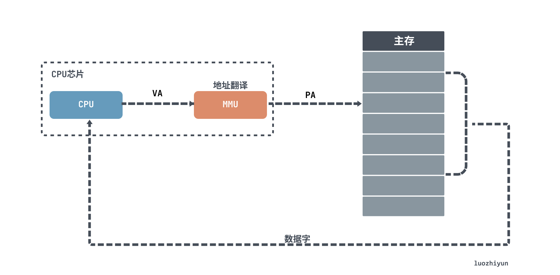
As shown above, when the CPU accesses the main memory, a virtual address is translated by the Memory Management Unit (MMU) into a physical address (PA) in order to access it.
The most intuitive way to map a virtual address to a physical address is to create a mapping table. This mapping table is called a Page Table in computer.
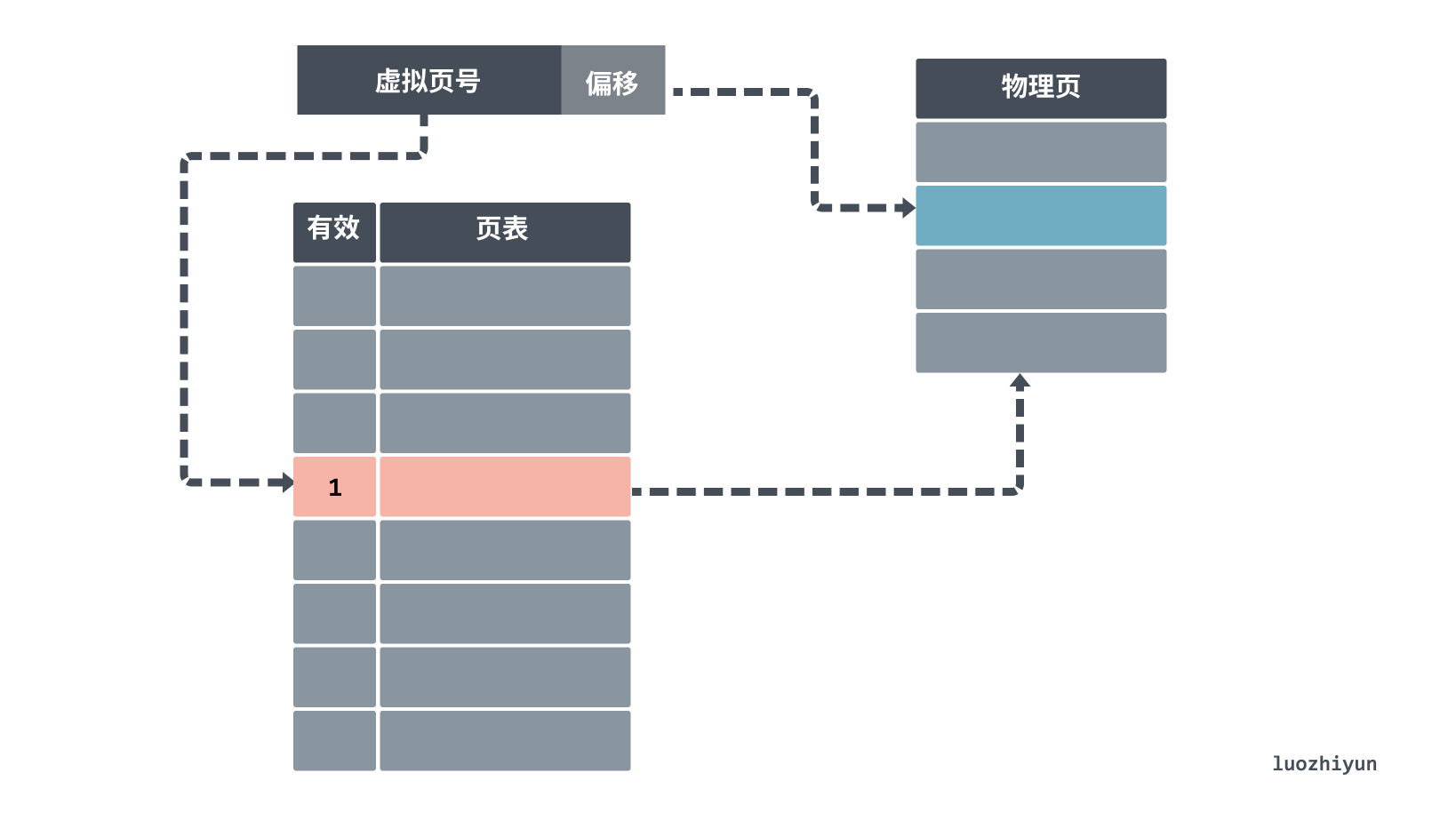
When looking up the page table, the virtual address is divided into two parts: the page number (Directory) and the offset (Offset). The first high bit indicates the page number of the memory address. The lower bit after that represents the offset inside the memory address.
The search method is similar to the group association mentioned above, first use the virtual page number as an index to find the corresponding physical page number in the page table, there will also be 1 bit in the page table indicating a valid bit, if the bit is invalid, it is not in main memory and a page miss occurs; if it is valid, then you can get the corresponding physical page number to get the corresponding physical page location, and then get the physical memory address according to the offset.
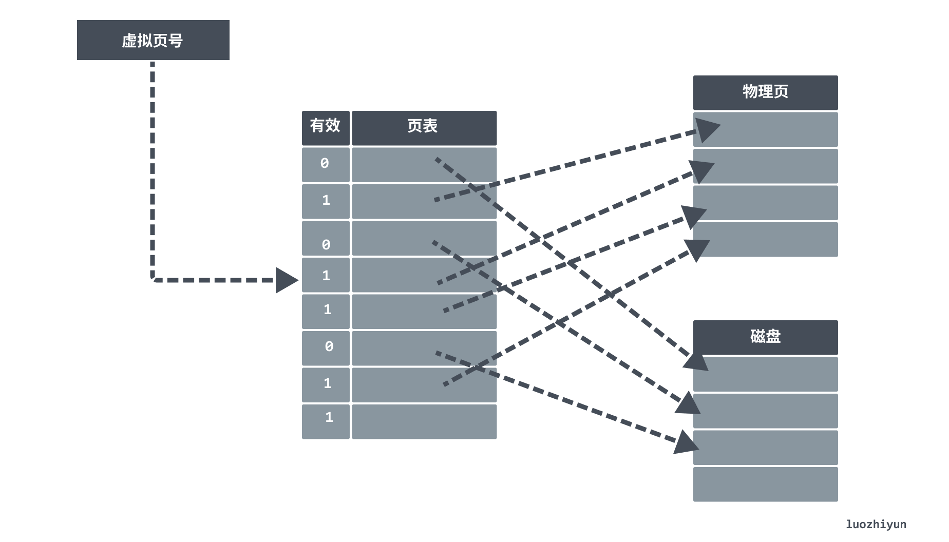
If the valid bit is off, then the page exists only at a specified disk address on the disk. A missing page triggers a missing page exception, and then the page is found in flash memory or on disk and placed into the main memory DRAM.
If the main memory is full, then a sacrificial page is selected and most operating systems will use the LRU replacement policy for page replacement. The operating system looks for the least used page and the replaced page is written to the disk’s swap partition (swap partition). swap partition, often referred to as a swap partition, is a special piece of hard disk space where the operating system removes a portion of temporarily unused data from memory and places it in the swap partition when there is not enough actual memory, thus freeing up enough memory space for the currently running program.
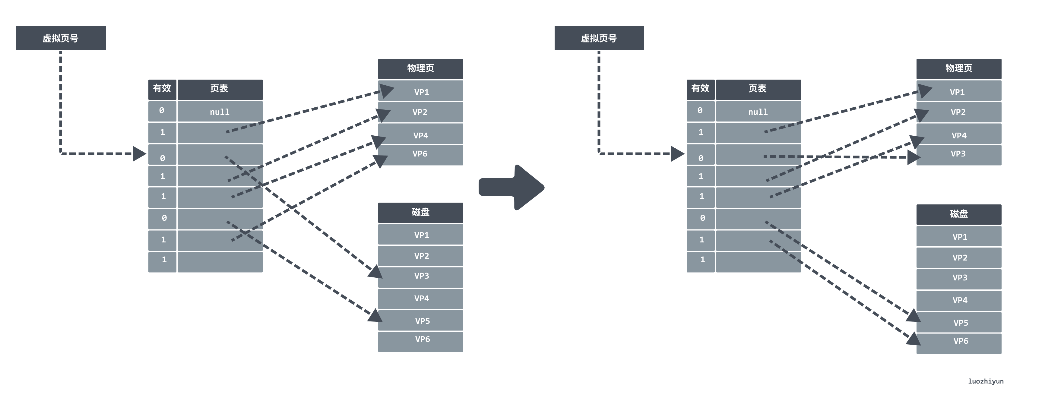
In the following figure assume that the VP6 stored in main memory is selected for replacement, replacing VP6 with VP3. If the replaced VP6 has already been modified, then the kernel copies it back to disk.
Due to locality, programs generally work on a small set of active pages, and the page switching overhead exists only when the program is dispatched into memory at startup, with page hits for the rest of the program. However, if the working set of code is too large and exceeds the physical memory size, then the pages will keep swapping in and out, generating jitter.
Multi-level page table
Suppose we now have a 32-bit address space, 4KB pages and a 4-byte PTE, then we need a 4MB page table resident in memory, and this page table is exclusive to each process, so it will cause a big memory waste, we need a way to optimize our page table space storage.
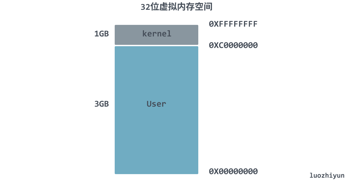
Think about the virtual memory space structure, the entire 4 GB space, the operating system uses 1 GB, from address 0XC0000000 to 0XFFFFFFFF, the remaining 3 GB left for user space, in fact, many programs do not use such a large space, for 64-bit systems, each process will have 256 TiB of memory space, that will be even less used.
So for the unused space, can we not load it into the page table and wait until the space is used before allocating a page table entry to it in the page table, can we not save a lot of space.
When the program is running, the memory addresses are allocated from the top down, constantly occupying the space of the stack. The heap, on the other hand, has memory addresses from the bottom to the top, which are constantly allocated and occupied. So, inside an actual program process, the address space occupied by virtual memory is usually two contiguous segments. The multi-level page table is particularly suitable for such a memory address distribution.
Assuming that the 32-bit virtual address space is divided into bits of 4KB per page and each entry is 4 bytes, then we can make each PTE (page table entry) in the first level page table responsible for mapping a 4MB slice of the virtual address space, which consists of 1024 contiguous pages, representing the second level page table. If the address space is 4GB, then 1024 level 1 page table entries can cover the entire space.
As shown in the figure below, the first 2K pages of memory are given to code and data, the next 6K pages are unallocated, in the next 1023 pages are also unallocated, and the next one page is allocated to the user stack.
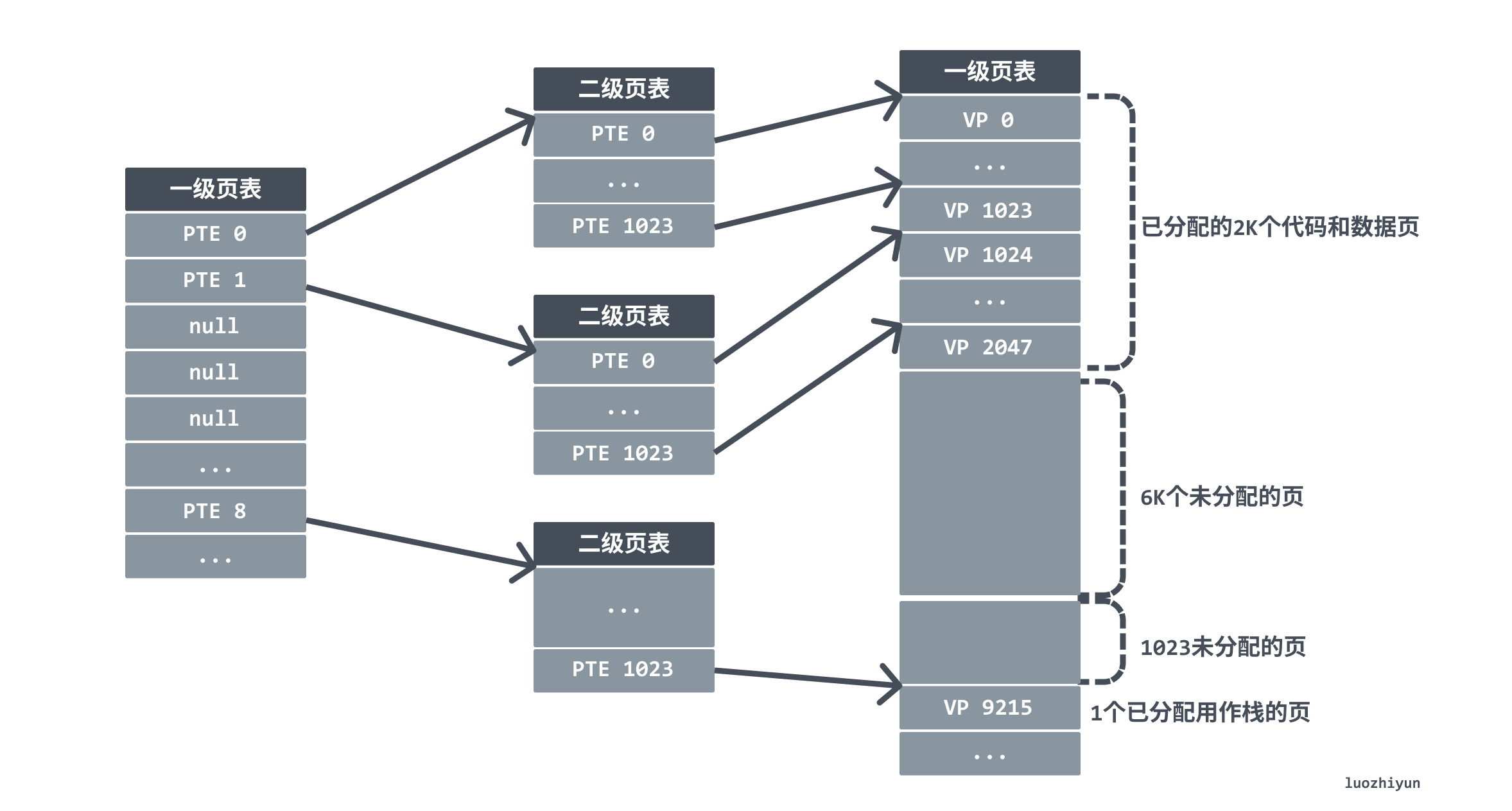
This approach reduces the memory footprint in two ways. First, if a PTE in the primary page table is empty, then the corresponding secondary page table will not exist at all. Since many programs actually occupy much less memory than the size that the page table can represent, a large space of page table entry resources can be saved. Second, only the primary page table needs to always be in main memory, the secondary page table will be created or destroyed when needed, and only the most frequently used secondary page table needs to be cached in main memory, which reduces the pressure on main memory.
Linux introduced four levels of page tables to aid in virtual address translation in 2.6.10.
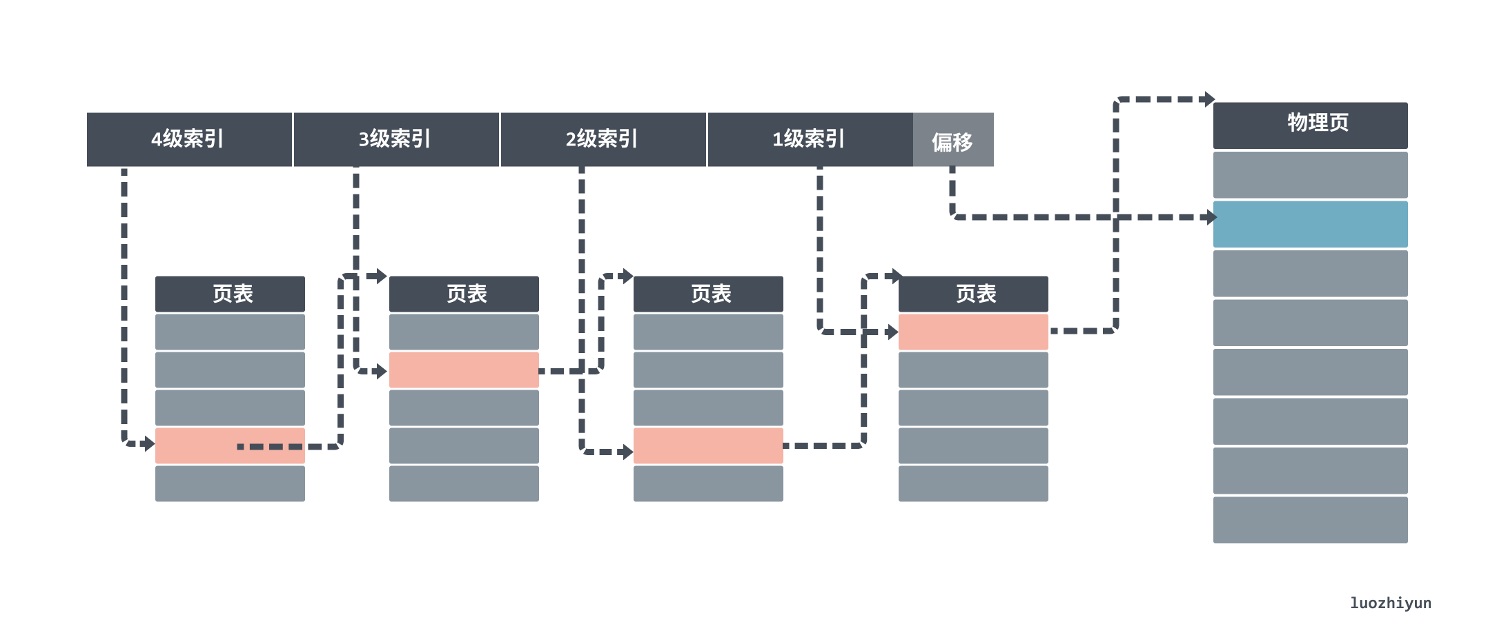
The first thing you will find is the entry in the level 4 page table. Each entry in a level 4 page corresponds to a level 3 page table, so we may have more than one level 3 page table.
Once we find the corresponding level 3 page table, we use the level 3 index to find the corresponding level 3 index entry. level 3 index entries then point to a level 2 page table. After getting the physical page numbers stored in the level 1 page table, we can also use the “page number + offset” method to get the final physical memory address.
TLB-accelerated address translation
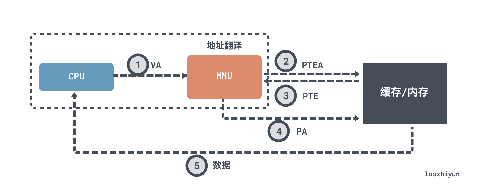
For a page hit data fetch process typically, without TLB acceleration it would look like this.
- the CPU generates a virtual address and passes it to the MMU.
- the MMU generates the page table entry address PTEA and requests the page table entry PTE from the cache/main memory.
- the cache/main memory returns the PTE to the MMU.
- the MMU constructs the physical address PA and passes it to the cache/main memory.
- the cache/main memory returns the requested data to the CPU.
A simple data fetch requires multiple interactions with memory, and if it is a 4-level page table, then it requires 4 accesses to memory to get the corresponding physical page number. In the case of missing pages, there is also a PTE swap or load process. As mentioned at the beginning, the performance of accessing memory is actually very low, and in fact it seriously affects CPU processing performance.
The instructions that the program needs to use are stored sequentially in the virtual memory. The instructions we execute are also executed sequentially one by one. In other words, there is “spatial locality” and “temporal locality” for accessing instruction addresses, as described in the previous sections, and the data to be accessed is the same. We have executed 5 instructions in a row. Since the memory addresses are contiguous, we can cache the addresses of the previous memory translations by adding a cache to reduce the interaction with memory.
The added layer is the cache chip TLB (Translation Lookaside Buffer), which holds a block consisting of a single PTE per line.
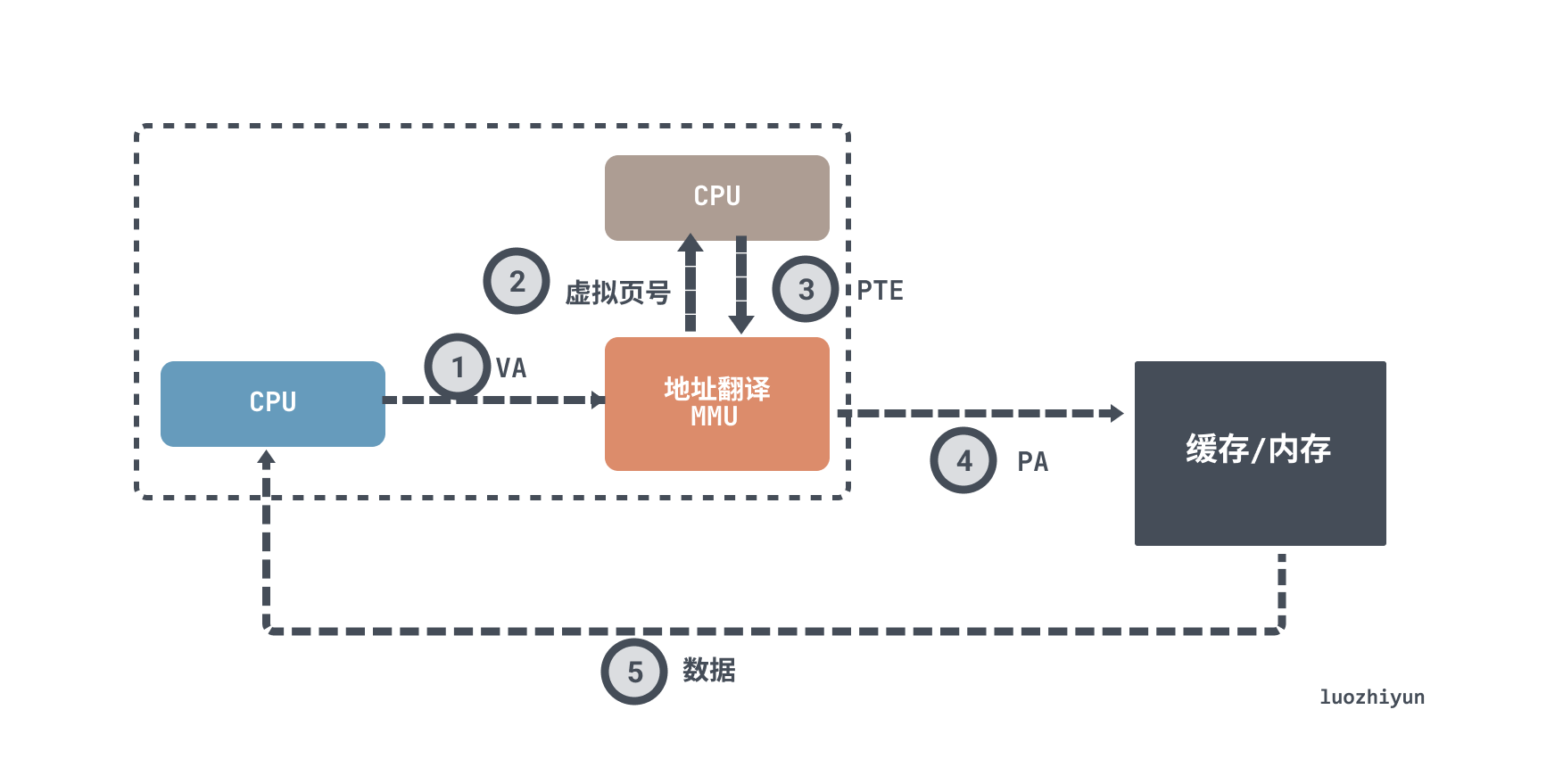
The process of querying data then becomes.
- the CPU generates a virtual address.
- the MMU retrieves the corresponding PTE from the TLB.
- the MMU translates this virtual address into a physical address and sends it to the cache/main memory.
- the cache/main memory returns the requested data word to the CPU.
Finally, let’s look at why virtual memory is needed
After talking about what virtual memory is, let’s finally talk about the need for virtual memory.
Since operating virtual memory is actually operating a page table, we know from the above explanation that the size of the page table actually has nothing to do with physical memory, and that when physical memory is not enough, you can use page misses to replace the needed data into memory, which only needs to hold the active part of the many programs, and does not need to load the whole program into memory, which allows machines with small memory to run programs.
Virtual memory can provide separate memory space for running processes, creating the illusion that each process’ memory is separate. Virtual memory space is simply a logical structure in the operating system that translates virtual addresses through a multi-layered page table structure that allows multiple processes to share physical memory through virtual memory.
And a separate virtual memory space will also simplify the memory allocation process. When a user program requests heap memory from the operating system, the operating system can allocate several contiguous virtual pages, but these virtual pages can correspond to non-contiguous pages in physical memory.
Then there is the provision of memory protection mechanisms. Any modern computer system must provide the operating system with the means to control access to the memory system. Pages in the page table in virtual memory hold read permissions, write permissions, and execute permissions. The memory management unit can determine whether the current process has permission to access the physical memory of the target, so that we end up converging all the functions of permission management into the virtual memory system, reducing the number of code paths that could be at risk.
Summary
From the above we can know that the CPU cache structure generally consists of L1, L2, and L3 cache structure. The CPU reads data only interacts with the cache and does not directly access the main memory, so a set of mapping relationships is maintained between the CPU cache and the main memory. When the data being looked up is missing, it needs to wait for the data to be loaded from main memory to the cache, and if the cache is full, then it also needs to be eliminated. If the eliminated data is dirty, then it needs to be written back to the main memory. The write strategies are write-through and write-back.
Since the CPUs in today’s computers are multi-core and cached data is shared by multiple cores, there are protocols like MESI to maintain a state machine to ensure that data is consistent across multiple cores.
In order to access data safely, easily, and quickly, a layer of virtual memory is added, and each program maintains a page table at startup, which maintains a set of mapping relationships; the CPU actually operates on virtual addresses, and each time the MMU needs to map the virtual addresses to physical addresses in the page table to find data. In order to save memory, a multi-level page table is designed, and a cache chip TLB is added to find data from the page table faster.
Reference
https://draveness.me/whys-the-design-os-virtual-memory/https://people.freebsd.org/~lstewart/articles/cpumemory.pdfhttps://www.luozhiyun.com/archives/701