On modern CPUs (most of them), all memory accesses need to go through layers of cache, and understanding the CPU cache update coherency issues can be of great help in designing and debugging our programs. This article will introduce the CPU cache system and how to use memory barriers for cache synchronization.
The memory hierarchy of early computer systems had only three levels: CPU registers, DRAM main memory, and disk storage. Due to the large performance gap between the CPU and main memory, the CPU had to wait a long time to read and write data, so an SRAM cache memory, called L1 cache, had to be inserted between the CPU registers and the main memory. As the performance gap between the CPU and main memory gradually increased, L2 and L3 caches were added gradually, and the access speed between CPU and Cache and Memory was roughly as follows.
- It takes 1 clock cycle to access CPU registers.
- It takes about 4 clock cycles to access the L1 Cache.
- Access to L2 Cache takes about 15 clock cycles.
- Accessing the L3 Cache takes about 50 clock cycles.
- Access to Memory takes approximately 200 clock cycles.
The performance gap between CPU and main memory is called the von Neumann bottleneck . When we access memory, we encounter many fragmented wait cycles. For example, due to the transfer characteristics of the level protocol, a certain amount of signal stabilization time is required before a row is selected, a column is selected, and reliable data is fetched. On top of that, since main memory uses capacitors to store information, it needs to periodically refresh what it stores in order to prevent information loss due to natural discharge, which can also introduce additional wait times. Some sequential memory accesses may be more efficient but also have some latency, while those random memory accesses consume more time.
It can be seen that the CPU is very slow to read and write data directly to the main memory and spends most of its time waiting for data transfer, so the CPU cache structure has been introduced.
Overview
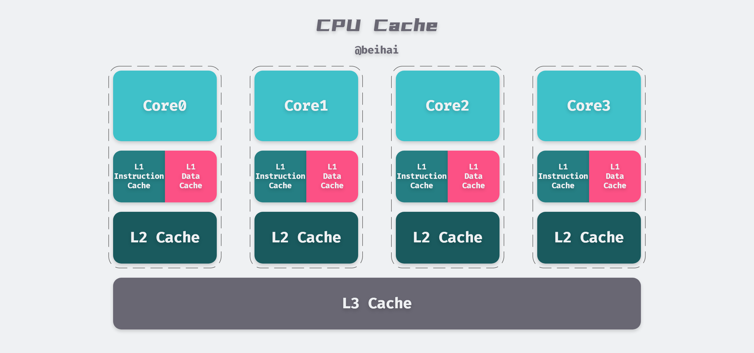
Most of today’s CPUs have three levels of cache. Take the 8265U I use as an example, its cache structure is as follows.
- Each CPU core has 64KB of L1 cache, of which 32KB is instruction cache and the other 32KB is data cache. L2 cache and L3 cache do not distinguish between instruction and data.
- Each CPU core has its own 256KB L2 cache, while the 6MB L3 cache is shared by all CPU cores.
- L1, L2, and L3 are faster and more costly the closer they are to the CPU, and slower the farther they are from the CPU.
The gradual increase in the number of cache levels also introduces two more important issues: one is the cache access hit problem, and the other is the cache update consistency problem. Before explaining these two issues, it is important to understand how the CPU reads and writes caches.
The CPU Cache and memory exchange data in cache blocks Cache Line, and the size of the Cache Line in today’s mainstream CPUs is 64Bytes, which is the smallest unit of data the CPU can get from memory. For example, if L1 has a 32KB data cache, it has 32KB /64B = 512 Cache Lines.
When the CPU sees an instruction to read memory, it passes the memory address to the first-level data cache. The first-level data cache checks to see if it has a cache block corresponding to this memory address. If it does, it is a cache hit, otherwise it loads the entire Cache Line from the second level cache.The CPU assumes that if we currently need data at a certain address, it is likely that we will immediately access its neighboring address, i.e., memory accesses tend to be localized, and once the cache block is loaded into the cache, the read instruction can proceed normally.
Cache Access Design
The data placement policy of the Cache determines where blocks of data in memory will be copied to the CPU Cache. Since the size of the Cache is much smaller than the memory, an address association algorithm is needed that can allow data in memory to be mapped to the Cache.
Fully Associative
Fully Associative means that data from any memory address can be cached in any of the Cache Lines. If a memory address is given, knowing whether it exists in the cache requires parallel comparison of the memory addresses in all Cache Lines. Therefore, the hardware design of Fully Associative is complex, requires an address comparator for each Cache Line, and is very expensive, so Fully Associative is not suitable for CPU caching.
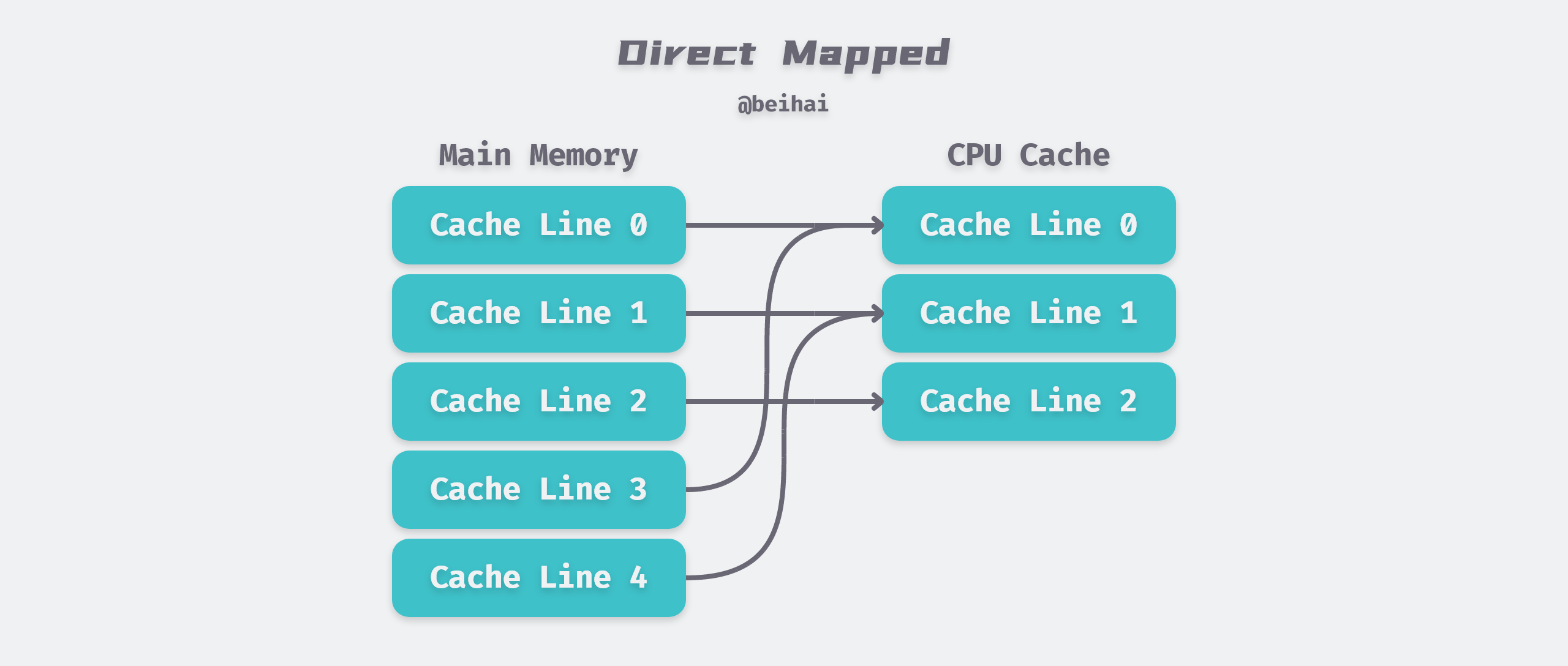
Direct Mapped
In order to reduce the linear growth of the direct search complexity, Direct Mapped was developed: it means that given a memory address, a unique Cache Line can be determined. since the data storage address under Direct Mapped is fixed and unique, it is prone to collisions, which eventually reduces the hit rate of the Cache and affects the performance.
Hash Table is the most common indexing method: the hash of the memory address is used as the Index of the array, and the value of the cached object is used as the Value of the array, and each time it is accessed, the address is hashed once and the corresponding location is found in the cache. Hashing is common in high-level programming languages, but it takes about 10,000 CPU cycles to compute a hash value, and for CPU Cache, the design goal is to get the data in a few dozen CPU cycles. If the access efficiency is tens of thousands of CPU cycles, it is better to fetch the data directly from memory.
To reduce the time required for access, we use a low time complexity algorithm such as modulo operation. If our L1 Cache has 512 Cache Lines, then the formula (address mod 512)* 64 will directly find the Cache location where it is located. However, this approach requires that the OS allocations and accesses to memory are nearly even in terms of addresses, otherwise the conflict situation would be very serious.
Contrary to our wishes, the operating system tends to use memory sequentially and centrally in order to reduce memory fragmentation and achieve convenience. This results in lower-numbered Cache Lines being allocated and used frequently, while higher-numbered Cache Lines are almost always idle because they are rarely accessed by processes. The waste caused by this situation further strains the already valuable CPU cache.
The flexibility of the die mapping is also not good enough. If you need to copy both block 0 and block 512 of main memory to Cache, even if other Cache Lines are free, they can only be copied to Cache Line number 0, which means they cannot be written to CPU Cache at the same time, and Cache Lines need to be erased and loaded continuously according to CPU execution process, which affects efficiency.
N-Way Set Associative
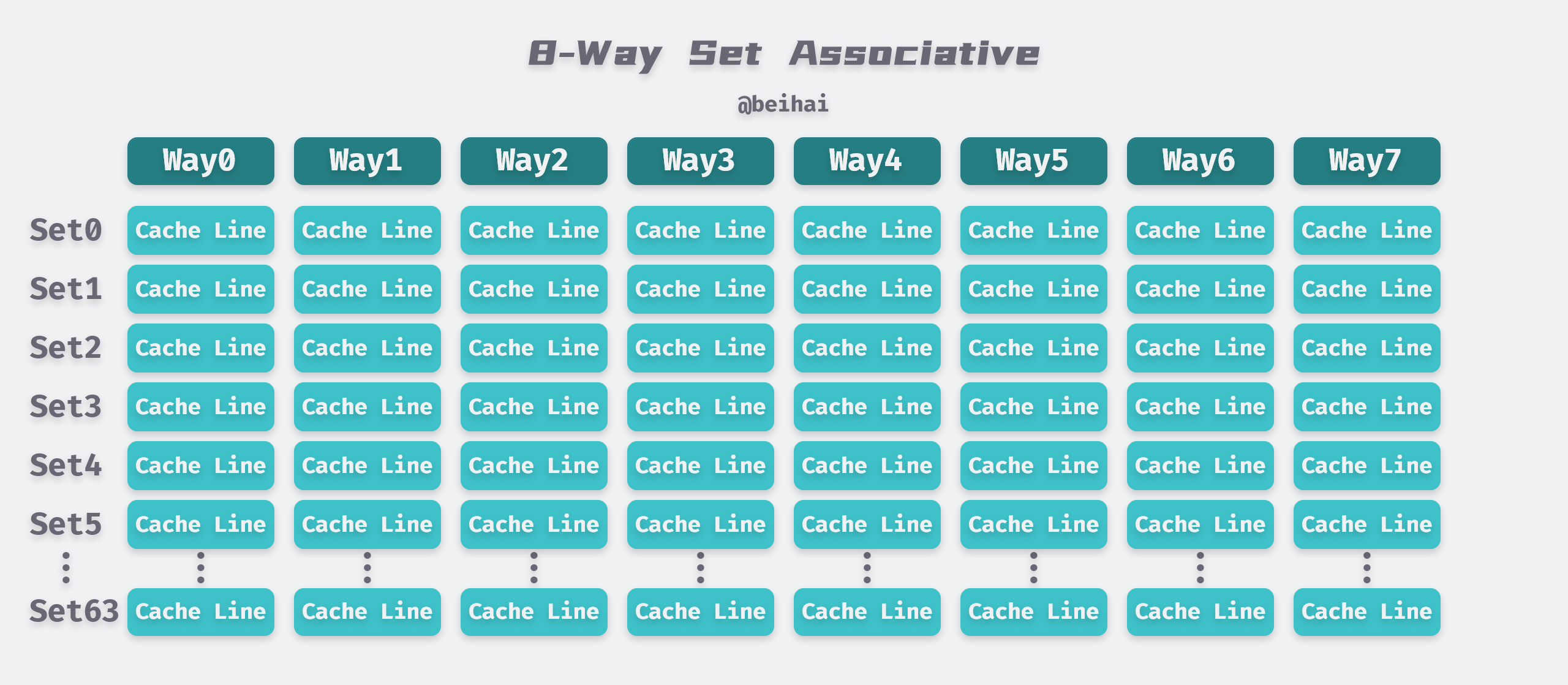
Set Associative is a trade-off between the above two options. The principle is that a cache is divided into a Set of N Cache Lines, and the cache is divided into equal groups, with the value of N usually being 4, 8, or 16, etc.
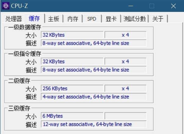
The above figure is a screenshot of the CPU-Z test I used, which shows that the different levels of cache use different N-Way set associations. To better understand the N-Way Set Associative, here is an example. Most Intel processors have a 32KB level 1 data cache, and a set of 8-Way (8 Cache Lines) association, each Cache Line is 64 Bytes, which means.
- 32KB can be divided into 32KB / 64 = 512 Cache Lines.
- Because there are 8-Way, there are 512 / 8 = 64 Sets.
- So each set has 8 x 64 = 512 Bytes of cache, and each Way has 4KB of cache.
Today’s operating systems divide physical memory into 4KB pages to be read, each with exactly 64 Cache Lines. When we read a memory page, these 64 Cache Lines are put into 64 Sets in sequence: the first Cache Line (Byte 0~63) is put into Set0, the second Cache Line (Byte 64~127) is put into Set1, and so on.
To facilitate indexing memory addresses, the Level 1 data cache uses a 36bits binary value to represent the address.
- Tag: the first 24 bits of each Cache Line address is a Tag, indicating the physical memory page to which it belongs.
- Index: the next 6bits are the Cache Line indexes in this Way, 2^6 = 64 just to index 64 Cache Lines.
- Offset: the last 6bits are used to indicate the offset in the Cache Line within the segment, 2^6 = 64Bytes.
- Valid: an extra binary bit to mark whether the Cache Line is valid or not.
Because each Set has 8 Cache Lines, it can hold multiple memory pages at once, which reduces the probability of cache collisions. The Index in the middle 6bits is used to locate the specific Set, then compare the Tag of the address with the Tag of the 8 Cache Lines in the Set in parallel, and if they are the same, the cache is hit (the Cache Line valid bit should be set to 1), and then get the specific data according to the Offset.

The memory address above is related to the specific addressing design of the CPU and is not the same concept as the virtual memory address of the operating system. The 36bits of memory address in the text can be used to represent 64GB of memory address, which means that the CPU supports up to 64GB of physical memory. The 64GB of physical memory can be divided into exactly 2^24 4KB memory pages, so 24 bits are used to store the Tag, which marks the memory page. In order to save space, the CPU is designed with a Cache that uses the exact number of bits to map RAM, mainly related to how much physical memory it plans to support, not 32bits/64bits as we often say.
Summary
In summary, the CPU cache can be represented as a tuple (S, N, B, m), i.e., each memory address has m bits, forming M = 2m addresses, and the Cache is organized as an array of S = 2s Cache Sets, each Cache Set containing N Cache Lines, each Cache Line containing B = 2b bytes of data blocks, Each Cache Line contains B = 2b bytes of data blocks, m-bit addresses, and one valid bit.
There are also many types of CPU Cache elimination policies, such as LRU, LFU and Random, and usually the CPU Cache elimination policy is LRU, which is not discussed in this paper.
Cache Coherence
In the previous section, we introduced the CPU cache read process. Nowadays, quad-core CPUs are common, and CPUs also need to ensure consistency between multiple physical core caches, which is somewhat similar to the consensus problem in distributed systems. However, CPU hardware does not need to consider network disconnections and delays, so the key to synchronization between multi-core CPU caches is how to manage the state of the data. Typically write operations are performed in the following two ways.
- Write Through mode: the write operation is written to both Cache and memory.
- Write Back: The write operation is written to the Cache and then flushed to memory asynchronously.
Because writing directly to memory is too slow, to improve write performance, mainstream CPUs use the Write Back strategy. Write-back mode has an additional advantage: it filters out repeated writes to the same address and ends up synchronizing to main memory only once. Also, if the cache segment works in Write Back mode, the system can erase a large swath of memory at a time instead of writing it in small chunks, which is more efficient.
Snoopy protocol
If a data x is updated on the cache of CPU core 0, the value of the data x on the cache of the other CPU cores should be updated as well. This problem is usually solved using the Snoopy Cache-Coherence Protocols: Snoopy protocols are more like a bus-type technology for data notification, whereby the CPU cache recognizes the state of data on other caches. If there is data sharing, the status of the shared data can be notified to other CPU Caches through a broadcast mechanism.
This protocol requires each CPU to be able to snoop the notification of data events and react accordingly. As shown in the figure below, there is a Snoopy Bus bus connecting the physical memory and the CPU Cache.
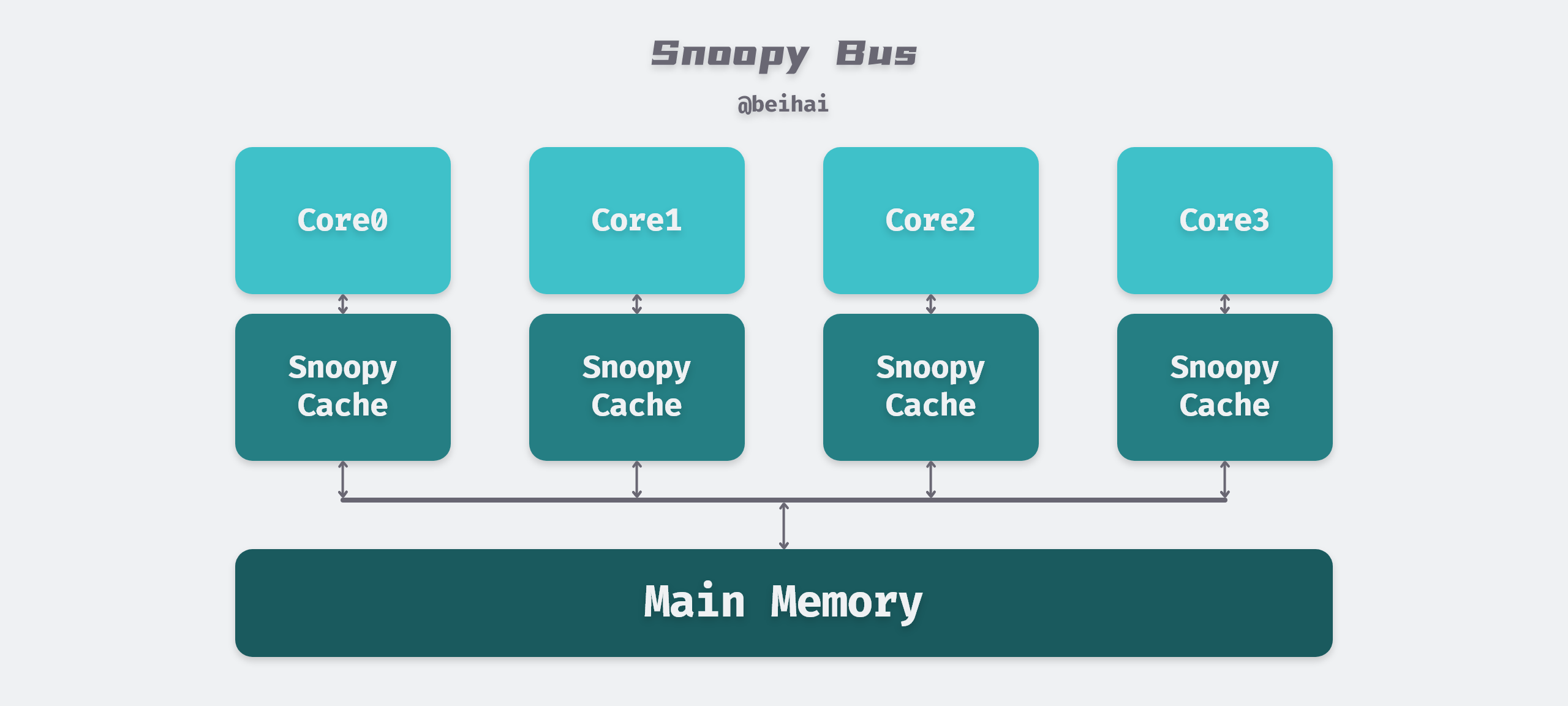
“The basic idea behind ‘snooping’ is that all memory transfers occur on a shared bus that is visible to all processor cores: the caches themselves are independent, but memory is a shared resource, only one cache can read or write memory in the same instruction cycle, and all memory accesses are subject to arbitration. Caches don’t just deal with the bus during memory transfers, but are constantly snooping around the bus to see what data is being exchanged and keep track of what other caches are doing . So when a cache goes to read or write memory on behalf of the core it belongs to, the other cores are notified as a way to keep their caches in sync. As soon as a processor writes memory, the other processors immediately know that the corresponding Cache Line in their own cache has been invalidated.
The reader may wonder why the L1 and L2 caches are not shared. This would avoid the cache synchronization problem. This is because the processor’s time when sharing the L1 cache is spent waiting in line to use the level 1 cache, at least once for each read and write instruction, which is very inefficient. Using multiple sets of caches and utilizing the cache coherency protocol makes them behave as if there is only one set of caches to meet the CPU’s speed requirements.
In addition to the Snoopy protocol, there is a Directory protocol, typically implemented by designing a centralized controller that contains global state information about the contents of various local caches. When a single CPU Cache makes a read or write request, this centralized controller checks and issues the necessary commands to synchronize and transfer data between the main memory and the CPU Cache or between the CPU Cache itself. Because of the centralized processing of data, this protocol has a higher latency, but it has better scalability in systems with many processors.
MESI Class Protocol
The MESI protocol is a write-failure cache coherency protocol and is the most commonly used protocol to support Write Back mode caching. In the MESI protocol, any one Cache Line has four different states.
- Exclusive: the Cache Line is only in the current cache and is clean (cached data is the same as the main memory data), when other caches read it, the status changes to Shared, and when the data is modified, it changes to Modified, and only the Cache Line in the Exclusive state can be modified.
- Shared: Cache Line also exists in other caches and is clean and can be discarded at any time.
- Modified: The Cache Line is Dirty and has a different value than the main memory. If other CPU cores want to read this data from the main memory, the Cache Line must be written back to the main memory and the status becomes Shared.
- Invalid: Cache Line is invalid and needs to be synchronized from main memory.
In the MESI protocol, only one CPU core is responsible for writing data. In the exclusive state, after this CPU core writes data to the Cache, it will broadcast a failure request to all other CPU cores to mark the corresponding Cache Line as invalid; while in the shared state, the same data exists in multiple CPU Caches, so it is necessary to broadcast a failure request to other cores to mark the Cache in other CPU cores as invalid before updating the data.
The MESI protocol marks other shared CPU cache data as invalid after the data is updated, and when the other CPUs read the data again, a Cache Miss occurs and the data needs to be updated from memory. Updating data from memory means a 20x speed reduction. If we could update directly from the CPU cache next door, this could increase the speed a lot, so there are extended versions of MOESI protocol and MESIF protocol.
The MOESI protocol, currently used by AMD’s CPUs, adds an additional Owner state to mark the source of the update data, and the Owner state is similar to the Exclusive state as a means of ensuring consistency between caches, but it allows the contents of dirty segments to be shared directly without first writing them back to memory.
The Forward state, added by Intel’s MESIF protocol, allows a clean Cache Line to be forwarded to another cache without the other cache having to re-read it from memory to get a shared copy. Both protocols make some optimizations to share data between caches to minimize latency.
Memory Model
We have understood the bus model and synchronization protocol of the CPU cache, and it is possible to obtain full sequential coherence if the CPU Cache can ideally satisfy the following conditions.
- the cache can respond quickly in the current instruction cycle as soon as it receives a bus event.
- the processor delivers the memory operation instructions to the cache in the program order and waits until the previous one is executed before sending the next one.
In practice, however, modern processors are always unable to meet the above conditions for various reasons.
- Cache will not respond to bus events in time: if a message is sent on the bus to invalidate a cache segment, but if the cache is processing something else at the time (such as transferring data with the CPU), the message may not be processed in the current instruction cycle and will enter the so-called ‘Invalidation Queue’, where the message waits in the queue until the cache is free for processing. Processors generally do not send memory operation instructions to the cache in strict program order: processors with Out-of-Order execution definitely do, but processors with in-order execution sometimes cannot fully guarantee the order of memory operations, for example, if the desired memory is not in the cache, the CPU does not stop working in order to load the cache, but instead performs instruction reordering. The write operation is particularly special because it is divided into a two-stage operation: before writing we first have to get exclusive access to the cache segment, and if we do not currently have exclusive access, we first have to negotiate with other processors, which also takes some time. By the same token, it is a waste of resources to leave the processor idle and doing nothing in this scenario. In fact, the write operation first initiates a request for exclusivity and then enters the Store Buffer queue, where the write operation waits until the cache is ready to process it.
These mean that, by default, read operations are likely to read obsolete data, such as corresponding failure requests that are still outstanding in the failure queue, and write operations are likely to actually complete later than their place in the code, and everything becomes ambiguous once chaotic execution is involved.
CPUs of different architectures provide different memory models, and machines of the ARM architecture have a relatively weak memory model: such CPUs have considerable freedom in reordering read and write instructions, and this reordering has the potential to change the semantics of programs in a multicore environment. This can be limited by Memory Barrier technology programs: Instruction reordering operations are not allowed to cross set boundaries. In contrast, x86 has a stronger memory model.
Instruction Rearrangement
Each CPU runs a program, and the execution of the program generates memory access operations. In this abstract CPU, memory operations are loosely ordered, and memory access operations are executed in their own convenient order without changing the speculation of the program execution results. For example, suppose there exists the value { A == 1 ; b == 2} and consider the result of executing the following instruction.
| CPU 1 | CPU 2 |
|---|---|
| A=3; | x=B; |
| B=4; | y=A; |
The four instructions above will have 24 combinations of memory access operations, each of which may occur and will ultimately produce four execution results.
|
|
Even more brutally, a write operation that has been committed by one CPU may not be sensed by another CPU and thus fetch the old value. Take for example the following example.
In addition, the CPU may also merge memory access operations, for example, the two address instructions X = *A; Y = *(A + 4); may be merged into either of the following execution sequences.
Memory Barrier
While the CPU can perform instruction reordering, it provides us with minimal guarantees.
- that memory access operations with dependencies are sequential.
- overriding load-store operations in the same CPU core are sequential.
If we want a higher level of instruction execution order that we can control in the program, we need to use memory barriers, and there are generally four common types.
- write barriers: write barriers ensure that any STORE operation that appears before a write barrier is executed before any STORE operation that appears after that write barrier, and write barriers are generally used in conjunction with read barriers or data-dependent barriers.
- Read Barrier: A read barrier ensures that any LOAD operation that appears before a read barrier is executed before any LOAD operation that appears after that read barrier; a read barrier is typically used in conjunction with a write barrier.
- Data Dependency Barrier: a data dependency barrier is a weak read barrier that is used between two read operations and where the second read operation depends on the first read operation (for example, where the first read operation obtains the address used by the second read operation), the read barrier is used to ensure that the target of the second read operation has been obtained by the first read operation, and the data dependency barrier can only be used where a data dependency does exist
- General Memory Barrier: the general memory barrier guarantees that all memory accesses that appear before the barrier (LOAD and STORE) are executed before memory accesses that appear after the barrier, like a combination of read and write barriers.
For example, in the following example, we use a write barrier and a data-dependent barrier to secure the values of B and Q so that only predictable results occur in the program.
There are many more scenarios for memory barriers, so it is impossible to describe their usage in detail in this article, but you can read the Linux documentation LINUX KERNEL MEMORY BARRIERS, most of the time we rarely use them directly, but knowing about them can help us understand the design of the program better.
Summary
In general, CPU Cache is transparent to software engineers, and all operations and policies are done inside the CPU. However, knowing and understanding the design idea and working principle of CPU Cache is beneficial for us to make better use of CPU Cache and write more CPU Cache-friendly programs. The author has also thought about some relevant application scenarios.
- Keeping the granularity of data comparison updates in CAS algorithms within the cache can further improve execution efficiency.
- The direct-write/write-back idea of Cache can be carried over to the database-buffer system in business scenarios to help us weigh the execution options.
- In suitable scenarios, ’locking’ the data at the CPU level reduces the performance loss of this process.
The cache coherency protocol in CPU Cache is similar to consensus in a simplified distributed system, and it is also an interesting process to look at this from a microscopic perspective. This also shows that some of the principles in computer science are similar, and although the knowledge is vast, it is important to learn to grasp the key points, and then you will be able to use them all.
References
- https://wingsxdu.com/posts/note/cpu-cache-and-memory-barriers/
- Cache coherency primer
- LINUX KERNEL MEMORY BARRIERS
- Cache: a place for concealment and safekeeping
- CPU cache knowledge relevant to programmers
- In-depth Understanding of Computer Systems, Section 6.4: Cache Memory
- What is the benefit of the MOESI cache coherency protocol over MESI?
- MESI protocol